China’s Memory Push Rattles Samsung, SK Hynix as ‘Golden Window’ Narrows
Forecast Trend Report by Period


YMTC patent portfolio outstrips Samsung and SK Hynix as China targets the post-HBM market
China steps up semiconductor self-reliance, narrowing memory technology gap with South Korea to about three years
YMTC holds 119 NAND patents, versus 94 combined for South Korean rivals
US curbs blocked imports of advanced chipmaking tools
China is using upgraded legacy processes to sidestep HBM bottlenecks
South Korea must secure irreplaceable technology, experts say
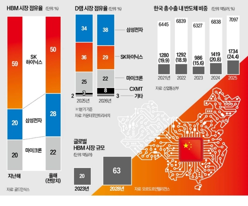
As recently as 2024, Chinese companies in the global memory-chip market were largely confined to low-cost commodity products. China’s share of the global DRAM market was so small it was not separately tracked at the time. In the first quarter of 2026, however, ChangXin Memory Technologies Inc., or CXMT, lifted its DRAM market share to 8%. The gain reflects Beijing’s push for semiconductor self-sufficiency despite tough US sanctions.
China is now aiming beyond commodity DRAM and into artificial-intelligence memory. It is accelerating development of high-bandwidth memory, or HBM, and next-generation architectures. Experts put the memory technology gap between South Korea and China at about three years, but China is closing in quickly. That is increasing pressure on Samsung Electronics Co. and SK Hynix Inc. to defend their technology lead.
South Korea’s dominance in HBM and DRAM faces pressure
China still trails South Korea in HBM development. Samsung Electronics and SK Hynix have moved beyond mass production of fifth-generation HBM3E and are now competing for leadership in HBM4. They plan to start mass production of HBM4E next year. China, by contrast, has faced major obstacles after US restrictions cut off imports of advanced extreme ultraviolet lithography systems from ASML Holding NV, equipment essential for the most advanced processes.
China has found a workaround. By deploying technologies including multi-patterning to upgrade older process nodes, it is bringing HBM development within reach. CXMT has shifted 20% of its production lines to HBM and is concentrating on HBM3 and HBM3E development.
The HBM technology gap between the two countries has narrowed to about three years from more than five, according to industry analysis. Choi Woo-young, a professor in the Department of Electrical and Computer Engineering at Seoul National University, said yields and stability could improve much faster than expected once Chinese AI-chip developers such as Huawei Technologies Co. begin adopting the products for domestic use and gain real-world experience.
Commodity DRAM is no safe haven either. China’s challenge is becoming more visible in DDR5, the main memory product used in the latest servers and PCs. Demand for Chinese-made chips is also rising as tight memory supply persists during the semiconductor boom.
CXMT is ahead in some next-generation technologies
Warning signs are already flashing in NAND flash. Samsung Electronics and SK Hynix lead higher-value markets such as enterprise solid-state drives, or eSSDs, with products in the high-200-layer to 300-layer range. But the move toward ultra-high-layer NAND above 400 layers has brought physical limits into focus. Wafer-to-wafer hybrid bonding has become essential. The process is an advanced packaging technology that vertically connects circuits by directly bonding two semiconductor wafers without conductive bumps between chips. China’s Yangtze Memory Technologies Co., or YMTC, has taken an early lead in the patent landscape for that technology.
YMTC was the first company to commercialize its proprietary Xtacking technology and has mass-produced products ranging from 160 layers to its latest 270-layer chips. It holds 119 core patents, compared with 83 for Samsung Electronics and 11 for SK Hynix as of 2023. Samsung, the global NAND leader, has signed a patent-licensing agreement with YMTC to develop triple-stack NAND for next-generation V10 products with more than 430 layers.
China is also stepping up work on next-generation technologies designed to overcome US restrictions. One of the most prominent is bonded DRAM. The technology forms the data-storage cell area and the control-oriented peripheral area on separate wafers before bonding them together. CXMT is known to be testing the technology on a bonded DRAM pilot line in Hefei. That approach would allow it to manufacture ultra-high-density DRAM using only deep ultraviolet equipment and multi-patterning, without EUV tools. Samsung is developing bonded DRAM through its B1b project. SK Hynix is doing the same. Even so, some industry observers say CXMT may be ahead of South Korea in both technology and speed.
China is also moving quickly in Compute Express Link, or CXL, DRAM, often described as the post-HBM market. Building on its mass-production experience in server-grade DDR5, CXMT has formally set its sights on the CXL 3.0 market. It is also expanding cooperation with Chinese fabless companies including Montage Technology to secure the controller technology central to the product.
Lee Byung-hoon, a professor in POSTECH’s departments of electrical engineering and semiconductor engineering, said South Korea’s edge in the global supply chain has depended heavily on tough US semiconductor restrictions on China. Before the golden window created by those sanctions closes, South Korean chipmakers must secure an irreplaceable lead in next-generation memory and packaging, he added.
Kim Chae-yeon, Hankyung reporter why29@hankyung.com
Kang Hae-ryeong, Hankyung reporter hr.kang@hankyung.com
Won Jong-hwan, Hankyung reporter won0403@hankyung.com

Korea Economic Daily
hankyung@bloomingbit.ioThe Korea Economic Daily Global is a digital media where latest news on Korean companies, industries, and financial markets.