SK Hynix Approves $39.2 Billion for Yongin, Cheongju Chip Plants
Summary
- SK Hynix said it approved a total investment of $39.2 billion in new plants for Yongin Y2 and Cheongju M17 to meet AI memory demand.
- The Y2 fab in Yongin will serve as a production base for next-generation DRAM including HBM, with construction set to begin in July 2027 and the first clean room scheduled to open in June 2029. Investment will continue through October 2031.
- The M17 fab in Cheongju is planned to meet surging NAND flash and eSSD demand, with construction set to begin in February 2027, the first clean room to open in December 2028, and investment to continue through April 2031.
Forecast Trend Report by Period


Board Approves Mid- to Long-Term Investment Plan
Construction on Yongin’s Y2 Fab to Start in July 2027
First Clean Room Planned for June 2029
$13.8 Billion to Be Invested in Cheongju NAND Base
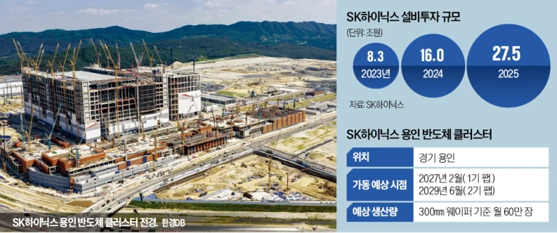
SK Hynix will invest a total of $39.2 billion to build new chip plants in Yongin and Cheongju as it moves to meet surging demand for artificial intelligence memory. The company aims to cement its position in the global AI supply chain by maximizing on-time supply capacity.
The board approved the investment plan on Aug. 7, allocating $25.4 billion to the Yongin Y2 fab and $13.8 billion to the Cheongju M17 fab.
The spending marks a key step in the company’s mid- to long-term investment strategy announced in June. SK Hynix is already pursuing a massive project that calls for $433.4 billion in the Yongin semiconductor cluster and $72.2 billion at its production base in Cheongju. Following the Y1 fab now under construction in Yongin, the company will simultaneously begin follow-up fabs in Yongin and Cheongju.
In the AI era, supply capacity is as critical as technological competitiveness because customers want the required volumes when they need them, a company official said. The company decided on the investment after closely reviewing market demand.
Yongin Y2 will be the second of four fabs planned for the Yongin semiconductor cluster. With a total floor area of 1,127,273 square meters, it will serve as a production base for next-generation DRAM, including high-bandwidth memory, or HBM. Construction is set to begin in July 2027, and the first clean room is scheduled to begin operations in June 2029. Investment will continue through October 2031. Construction of Y1, whose clean room is due to open in February 2027, is also progressing smoothly.
SK Hynix has brought forward the target completion date for the Yongin cluster to 2033 from 2045. Starting construction on Y2 is a key part of that roadmap. The first-phase infrastructure at the cluster site in Wonsam-myeon, Yongin, is 99% complete, paving the way for Y2 construction to proceed without disruption.
Cheongju M17 will be built to meet rapidly rising demand for NAND flash. Orders for enterprise solid-state drives, or eSSDs, are surging as AI services spread, while demand for NAND is also climbing sharply with the growth of AI inference and the emergence of agentic and physical AI. Cheongju already houses the M11, M12 and M15 NAND fabs, and SK Hynix plans to link M17 with those plants to improve production efficiency and speed construction of the new fab. M17 will have a total floor area of 680,992 square meters. Construction is scheduled to start in February 2027, and the first clean room will open in December 2028. Investment will run through April 2031.
SK Hynix said the investment should help secure future growth engines, strengthen South Korea’s semiconductor ecosystem and support regional economies. The company called the move a preemptive decision to avoid missing market growth opportunities and said it aims to build a stable AI semiconductor supply chain and establish itself as a key partner in global AI infrastructure.
Kim Chae-yeon, Hankyung.com reporter why29@hankyung.com

Korea Economic Daily
hankyung@bloomingbit.ioThe Korea Economic Daily Global is a digital media where latest news on Korean companies, industries, and financial markets.