Samsung Unveils 3D zHBM Claiming Up to 8x HBM5 Performance in Bid to Rebuild Chip Edge
Summary
- Samsung Electronics said it unveiled zHBM, zNAND-O and V10 BV-NAND to address rising demand for high-performance computing and AI infrastructure.
- Samsung said zHBM is targeting up to 8x the performance of HBM5, a 3x improvement in performance per watt, and less than half the thermal resistance as it seeks to maximize AI system performance and power efficiency.
- Industry sources and Samsung officials said the technologies signal a push to restore fundamental competitiveness and secure leadership in memory and NAND through 3D packaging, HCB, thermal management, foundry and on-device AI.
Forecast Trend Report by Period


Samsung unveils vertically stacked 3D HBM
zHBM targets up to 8x HBM5 performance, aiming to break stacking limits
Up to 3x better power efficiency and less than half the thermal resistance of HBM5
Shorter data paths help ease bottlenecks
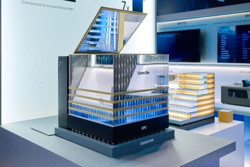
Competition in memory for artificial-intelligence chips is evolving from making it faster to bringing it closer. Samsung Electronics has unveiled zHBM, a next-generation 3D memory architecture that stacks high-bandwidth memory directly on top of an AI accelerator, along with zNAND-O, an ultra-high-layer NAND flash technology with more than 400 stacked layers.
Samsung Bets on the Z Axis by Putting HBM on Top Instead of Beside
According to industry officials on Aug. 8, Samsung recently unveiled its next-generation 3D memory architectures, zHBM and zNAND-O, for the first time at FMS 2026, a memory and storage industry exhibition and conference held at the Santa Clara Convention Center in California.
The technologies are designed to meet rising demand for high-performance computing and AI infrastructure while maximizing AI system performance and power efficiency. They mark a shift from 2.5D packaging, which uses planar horizontal and vertical space, to 3D packaging that also uses the height dimension, or Z axis. That is why the products carry the "z" name.
Academic researchers view zHBM as a meaningful break from conventional chip placement. Until now, HBM has typically been positioned beside AI accelerators such as graphics processing units, exchanging data laterally. zHBM instead stacks memory vertically on top of the AI accelerator itself.
When a GPU takes longer to fetch data from memory, the entire system slows. That is why data movement between memory and GPUs has emerged as a new bottleneck in AI chips.
HBM was originally developed to address that problem. It stacks multiple DRAM chips vertically and links them through tiny vertical channels known as through-silicon vias, or TSVs, allowing far more data to be transferred at once than with conventional DRAM. Even so, standard HBM sits next to the GPU and is connected across separate chips, limiting how wide the data path can become.
zHBM reverses that structure. If conventional HBM is like building a warehouse next to a GPU, zHBM is like stacking the warehouse directly above it. That sharply reduces the distance data must travel.
Samsung is focused on that shorter path. A shorter distance can reduce signal loss and cut the power needed to move data. It can also enable denser connections between memory and the accelerator, increasing throughput.
Samsung said zHBM could deliver as much as eight times the performance of HBM5 and improve performance per watt by as much as three times. The company also said thermal resistance could be reduced to less than half that of HBM5. Rather than simply increasing HBM speed, Samsung is trying to improve performance and power efficiency at the same time by changing the connection structure between memory and compute.
A key technology is Hybrid Copper Bonding, or HCB. To stack multiple HBM layers on top of an accelerator, each DRAM chip must be connected at extremely high density. Existing approaches have relied on microbumps to link chips.
HCB directly bonds chip surfaces using copper. That allows smaller, denser connection points and makes it easier to secure more data channels in the same area. Put simply, if the old method connected two buildings with several small bridges, HCB places the buildings almost flush together and greatly widens the passageways.
The challenge is heat. In semiconductors, how quickly heat can be removed helps determine performance limits. As temperatures rise, chips can throttle to maintain stable operation. Stacking HBM on top of a GPU shortens the data path, but it also makes heat harder to dissipate because the GPU already generates substantial heat and the memory above it operates at high speed.
It is similar to placing one hot stove on top of another. Samsung presented a concept to address that issue through a heat-dissipation structure that moves heat outward through a separate path. The idea is to secure a heat-transfer route between the HBM and the AI accelerator so heat generated by 3D stacking can be removed efficiently. Samsung said zHBM's thermal resistance could be reduced to less than half that of HBM5.
Data movement is becoming increasingly important in AI chips as AI models grow larger and the amount of data that must be fetched from memory surges. In inference, the growth of the KV cache, which stores prior context from the model, means memory capacity and bandwidth are no longer the only issues. How efficiently data can be moved with minimal power is also becoming critical. That could change the basis of HBM competition.
An engineer familiar with the matter said DRAM process technology, stack count, TSVs, bandwidth and yield have been the key factors until now. Going forward, 3D packaging, HCB, thermal management, power delivery, logic processes and co-design with AI accelerators will also matter. Samsung, which has capabilities in memory, foundry manufacturing and advanced packaging, could gain an advantage through a one-stop ability to design and optimize AI accelerators and memory together from the outset, the engineer added.
Samsung Also Pushes NAND Higher With zNAND-O
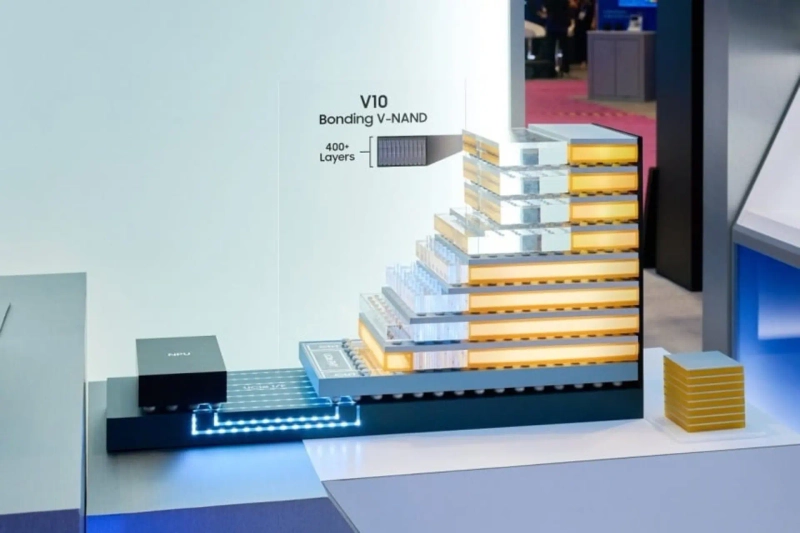
Samsung's NAND solution unveiled alongside the products also drew attention. zNAND-O is a high-performance NAND product optimized for on-device AI, which runs AI directly on devices. It uses TSV technology, which connects the upper and lower parts of a chip through microscopic holes, to support real-time ultra-fast data processing.
Samsung also unveiled its 10th-generation V-NAND, or V10 BV-NAND, built with more than 400 vertically stacked layers, reinforcing its lead in NAND technology. V10 BV-NAND uses wafer bonding, which vertically joins two or more wafers, and a three-stack technology that connects three NAND bundles. Samsung said that increased the amount of data that can be stored in the same area by about 58% from the previous generation, V9, while also improving read and write performance and speed.
The company also showcased an HBM5 model incorporating a new thermal-management technology called Hidden Path Block, or HPB, and a low-power double data rate 5X-based processing-in-memory, or PIM, product that performs calculations directly inside memory. Those offerings are aimed at high-performance computing and AI data centers.
A Samsung official familiar with internal matters said the technology announcement marked an opening signal in restoring the fundamental competitiveness that Vice Chairman Jun Young-hyun, who also heads the Device Solutions division, emphasized in 2024.
Kang Kyung-ju, Hankyung.com reporter qurasoha@hankyung.com

Korea Economic Daily
hankyung@bloomingbit.ioThe Korea Economic Daily Global is a digital media where latest news on Korean companies, industries, and financial markets.