TSMC Building 20 Fabs but Short of Construction Workers; What It Means for Samsung Electronics [Kang Kyung-ju’s TechX]
Forecast Trend Report by Period


TSMC Says Chip Demand Has Surged to Levels Unseen in 30 Years
Even After Structures Go Up, Clean Rooms and Specialty Gas Systems Still Must Be Installed
“Samsung Also Knows It Is Critical to Attract Skilled Fab Workers”
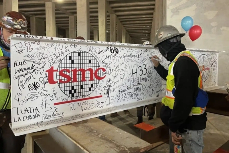
Taiwan Semiconductor Manufacturing Co., the world’s largest contract chipmaker, said it is building about 20 fabs worldwide at the same time but is still struggling to keep up with explosive artificial intelligence-driven demand. It cited a shortage of skilled construction workers, rather than funding, as the key bottleneck.
On Sept. 5, citing industry sources, Hou Yongqing, a senior vice president at TSMC and chairman of the Taiwan Semiconductor Industry Association, said at the CEO Summit at Semicon Taiwan 2026 in Taipei that the company is building about 20 fabs globally but still cannot meet demand. He said the semiconductor industry is facing a demand surge not seen in the past 30 years and estimated that equipment purchasing demand in July jumped 1.9 times from the end of last year.
“I have never seen demand change this sharply or this frequently in the past 30 years,” Hou said. Fab expansion had traditionally been built around long-term demand forecasts, with facilities and equipment added accordingly. Now demand is being reset within a single quarter, throwing equipment ordering plans into flux.
The scale of the buildout is also different from the past. Hou said TSMC is simultaneously advancing 13 wafer fabs in Taiwan and five to six overseas. That puts the total at about 20 sites under parallel construction worldwide. In the past, the company could handle only four or five projects at a time, but now it is expanding at four to five times that pace and still cannot satisfy demand.
At its earnings briefing on July 16, TSMC said it would build 13 leading-edge process and advanced-packaging fabs in Taiwan over several years. Hou’s latest remarks confirm that construction is under way and that, including overseas projects, the number of concurrent worksites has reached about 20.
Even so, Hou said tight supply reflects conditions at construction sites rather than a shortage of capital. After a fab’s structure is completed, clean rooms, specialty gas systems, maintenance infrastructure and front-end production equipment still must be installed. He identified construction labor as the most immediate constraint. Taiwan and Arizona both face shortages of skilled workers, and equipment installation remains even after the buildings are finished.
Hou called the severe shortage of construction labor the biggest obstacle to expanding production. Taiwan and the US are facing the same situation. He added that manufacturers are moving aggressively to introduce AI into production lines to boost capacity and prevent leakage of technology secrets.
At its July earnings briefing, TSMC raised its 2026 capital spending plan to $60 billion to $64 billion from $52 billion to $56 billion. It also added $100 billion to its US investment plan, bringing the cumulative total to $265 billion. If the earlier message was about stepping up investment, the latest remarks suggest equipment demand and on-site execution are nearing their limits as that money is deployed.
For equipment, materials and construction companies, that opens the door to additional orders. For fabless chip designers such as Nvidia and AMD that share TSMC’s manufacturing capacity, it means supply relief is unlikely in the near term for leading-edge nodes and for CoWoS, TSMC’s advanced packaging technology that integrates multiple chips into a single package.
“How the entire ecosystem can handle demand for output that has nearly doubled in just six months is the capacity challenge we face today,” Hou said.
The foundry market grew 29% from a year earlier as orders tied to AI semiconductors surged and production capacity was reallocated. Counterpoint Research said in a report published on Aug. 28 that the foundry market expanded 29% year on year.
Supply-demand imbalances persisted across both advanced and mature process nodes, the report showed. TSMC retained a dominant 73% share of the foundry market for a second straight quarter, supported by volume production of its 2-nanometer process, expansion of its 3-nanometer line, and tight supply in 8-inch and 12-inch mature-node production as well as advanced packaging.
An executive at a large construction company involved in building semiconductor fabs in South Korea said securing skilled workers to build clean rooms, mechanical, electrical and plumbing systems, and utility infrastructure would be critical if Samsung Electronics expands fab investment. Even after construction ends, a production line cannot begin operating until tool hook-up and yield stabilization are completed.
The executive added that Samsung also understands the importance of attracting skilled semiconductor fab workers. The company is devoting company-wide resources to building a workforce and partner ecosystem across the full process, from engineering, procurement and construction to equipment hook-up, commissioning and production ramp-up.
Kang Kyung-ju, Hankyung.com reporter (qurasoha@hankyung.com)

Korea Economic Daily
hankyung@bloomingbit.ioThe Korea Economic Daily Global is a digital media where latest news on Korean companies, industries, and financial markets.